Ultra-high density flash over 10Gbit / mm2 appears at ISSCC in February
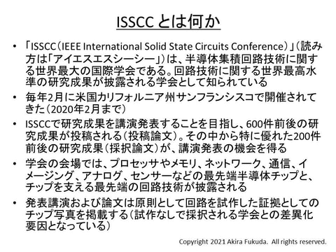
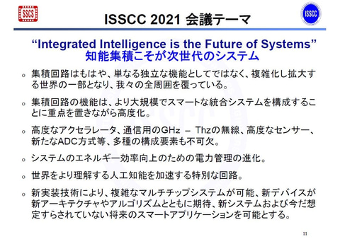
The world’s largest international conference “ISSCC (International Solid-State Circuits Conference)” will be held in February this year (2021), where the latest technology of semiconductor integrated circuits will be shown. In November of last year (2020), an outline of the event was explained at an online press conference, and after that , the detailed program became available for download in PDF format on the official website .
The ISSCC has been customary in recent years to be held every February at the Marriott Marquis Hotel in San Francisco, California, USA. The ISSCC in February last year (2020) was held as a real event at the same venue, partly because the effects of COVID-19 (new coronavirus infection) were mostly limited to China . However, this year (2021), the ISSCC is the first virtual conference due to the global pandemic of COVID-19.
At an international conference, a short paper (“submitted paper” or “abstract”) summarizing the research results is first sent to the secretariat of the society. In the treatise selection committee of the academic society, multiple selection committee members (experienced researchers) give evaluation points to the submitted papers, and the submitted papers with high evaluation points have the opportunity to present their lectures at the academic society. This paper (adopted paper) is included in the collection of papers of the academic society. In some academic societies, the submitted paper is in the same format as this paper, and the submission of this paper is omitted.
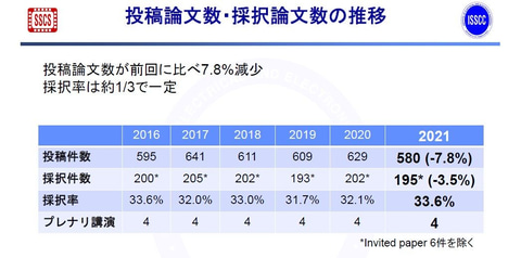
The ISSCC is known as the most prestigious international conference on semiconductor circuit technology. One of the factors that determine the format of international conferences is the acceptance rate (number of accepted papers / number of submitted papers). Academic societies with an acceptance rate of 50% or less are generally considered to be fairly prestigious. The adoption rate of the ISSCC has been around 33% in recent years, which is quite low. The fact that it is adopted means that the research results have gained a certain degree of evaluation.
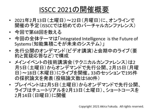
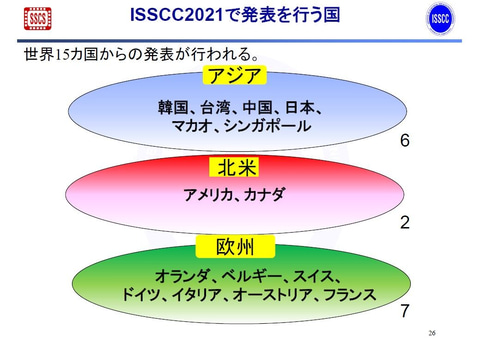
Of course, the format of the academic society does not determine only the acceptance rate. Years of effort and ingenuity by generations of stakeholders have maintained the status of the most prestigious academic society in the semiconductor circuit research community. By the way, the number of submitted papers for the 2021 ISSCC was 580, the number of accepted papers was 195, and the acceptance rate was 33.6%.
Video of technical lecture will be released in advance from February 5th
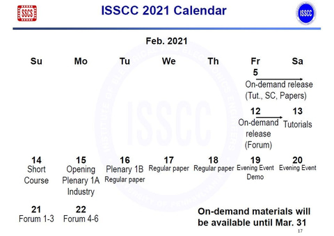
This year’s ISSCC will consist of a pre-release video lecture “On Demand” and a real-time event “Live” during the session. The main event technical lectures (lecture sessions, demonstration sessions, etc.) and pre-event technical lectures (tutorials and short courses) will be held on Friday, February 5, 2021 at 5 pm PST. Will start pre-release on Saturday, February 6th at 10am). The post-event lecture (forum) is scheduled to begin pre-release on Friday, February 12, the same year at 5 pm (US Pacific time, Japan time is Saturday, February 13 at 10 am). The on-demand viewing deadline is currently March 31, 2021.
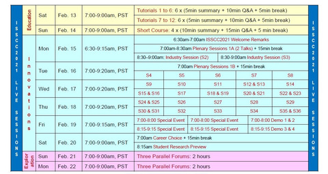
The technical lecture (technical conference) will be live from February 15th (Monday) to February 20th (Saturday), 2021. Both are in the morning time zone of US Pacific time, 6:30 am on February 15 (11:30 pm on the same day in Japan time) or 7:00 am on February 16-20 (Japan time). It starts at midnight the next day).
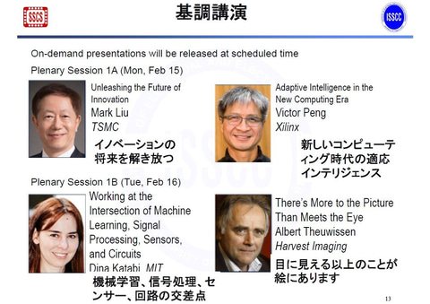
The annual keynote speech (Plenary Lecture, Session 1) will not be released in advance. A total of 4 live lectures are scheduled, 2 on February 15th and 2 on February 16th. Two talks on the 15th are TSMC’s Mark Liu on the future of innovation and Xilinx’s Victor Peng on the future of computing.
On the 16th, Dina Katabi of MIT (Massachusetts Institute of Technology) will give a lecture on machine learning and signal processing, sensors, and circuit intersections, and Albert JP Theuwissen of Harvest Imaging will give a lecture on the future of CMOS image sensors. After the live lecture, you will be able to watch the video of the plenary lecture on demand.
Invited talks on millimeter-wave 5G chips and motion detection chips
From here, let’s introduce the notable lectures of the technical lecture (technical conference). First of all, I would like to pay attention to the session in which semiconductor manufacturers and electronic equipment manufacturers report the technical outline of semiconductor chips developed and commercialized by invited lectures. An invited talk session called “Invited Industry Track” or “Highlighted Chip Releases”, and a similar session was set up at the previous ISSCC (ISSCC 2020). This time, there will be 6 invited talks in total, 3 each for “5G and Radar Systems” in Session 2 and “Modern Digital SoCs” in Session 3.
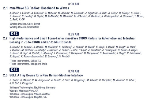
In Session 2, Analog Devices will provide a technical overview of chipsets for 5th generation (5G) mobile phone systems (lecture number 2.1). The lecture will include technology for converting between baseband and millimeter waves and millimeter wave beamforming technology. Texas Instruments will then introduce automotive and industrial millimeter-wave radar chips (lecture number 2.2). It is a single-chip sensor using RF CMOS technology, and has a radar chip in the 76GHz to 81GHz band and a radar chip in the 57GHz to 64GHz band.
Infineon Technology and Google will jointly report a technical overview of the chip “SOLI” that detects human movements (gestures) with millimeter-wave radar (lecture number 3.3). The Android smartphone “Google Pixel 4” released by Google in Japan in October 2019 is equipped with “SOLI” and is used as one of the sensors that make up the smartphone operation function “Motion Sense” by gestures. There is .
Invited talks on SoCs and high-end GPU chips for the latest Xbox machines
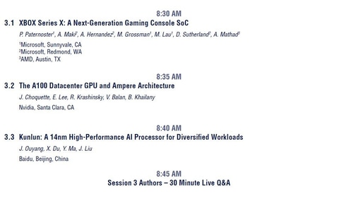
In Session 3, we will explain the technical outline of SoC (System on a Chip) jointly developed by Microsoft and AMD for the latest stationary video game device “Xbox Series X” (lecture number 3.1). The developed SoC incorporates eight custom CPU cores based on AMD’s “Zen 2” architecture and custom GPU cores based on AMD’s “RDNA 2” architecture .
NVIDIA will give a technical overview of the high-end GPU “NVIDIA A10” for data centers with Ampere architecture (lecture number 3.2). It is equipped with 3,456 CUDA cores for 64-bit floating-point arithmetic, 6,912 CUDA cores for 32-bit floating-point arithmetic, and 432 Tensor cores for deep learning arithmetic.
Baidu (Baidu ) reports the technical outline of the deep learning processor “Kunlun” (lecture number 3.3). It supports both cloud and edge solutions and achieves 260TOPS processing speeds with 100W of power consumption.
Presented adopted papers in 33 lecture sessions
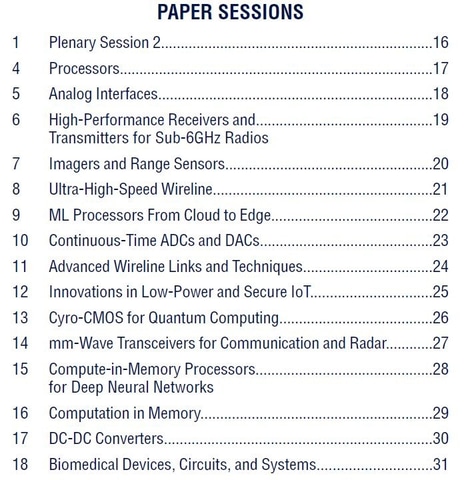
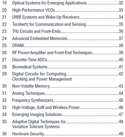
The 33 sessions from Session 4 to Session 36 will be the lecture presentation sessions (general lecture sessions) of the accepted papers. Until the last time, the session number and the presentation date were related, but this time you can watch the lecture video on demand, so the session number is not related to the order of the lectures. As in the past, live events are scheduled for earlier sessions with lower numbers and later sessions with higher numbers.
5nm CMOS chip that decodes 8K UHD images at 30fps
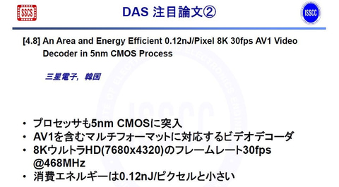
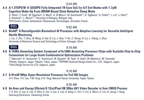
From here, I would like to introduce the notable presentations of the general lecture. Let’s start with Session 4, which has a processor theme. In this session, Samsung Electronics will present an 8K (UHD, 7,680 x 4,320 pixel) compatible video decoder LSI manufactured by 5nm generation CMOS technology (lecture number 4.8). When the operating frequency is 468MHz, UHD frames (screens) compressed with AV1 (AO Media Video 1) code can be decoded at 30fps. The energy required for 1-bit processing is as low as 0.12nJ.
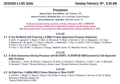
MediaTek will showcase the development results of an application processor for 5G mobile phone terminals manufactured in 7nm generation CMOS (lecture number 4.1). Similar to the existing application processor developed by the company, it adopts a “Tri-Gear” configuration equipped with three types of CPU cores with different characteristics such as “high speed”, “low power consumption”, and “intermediate (balanced)”. The operating frequency is 3GHz.
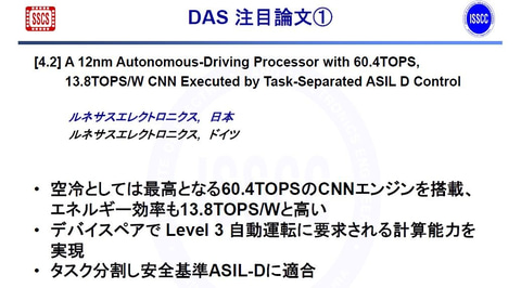
From Japan, Renesas Electronics will announce a processor for autonomous driving (lecture number 4.2). The processing speed of the built-in convolutional neural network (CNN) processing engine is 60.4 TOPS, and the processing speed per power consumption is 13.8 TOPS / W.
Further improvement of storage density of 3D NAND flash
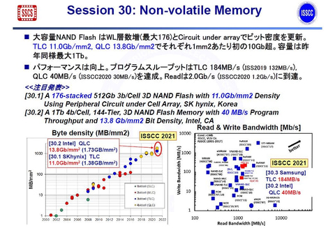
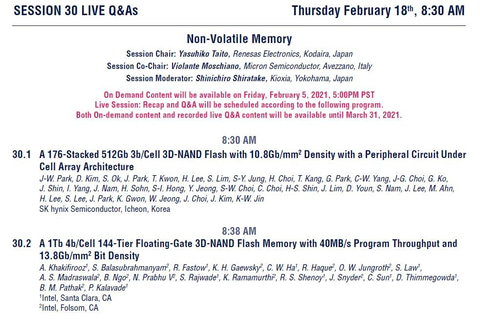
Next, I would like to focus on session 30 with the theme of non-volatile memory. The session will be followed by ultra-dense 3D NAND flash memory technology from five major NAND flash memory vendors. The storage capacity per square mm exceeded 10 Gbit. The storage capacity is stagnant near 1 Tbit, and the movement to increase the capacity is slow. It can be seen that the reduction of manufacturing cost per storage capacity is the highest priority.
SK Hynix announces 3D NAND flash technology with 176 layers of memory cells (lecture number 30.1). It uses 3bit / cell (TLC) multi-value storage technology. The storage capacity of the prototype silicon die is 512 Gbit. The storage density reaches a record high of 10.8 Gbit / mm2 for the TLC method.
Intel has developed a 3D NAND flash technology with 144 layers of memory cells (lecture number 30.2). It uses a 4-bit / cell (QLC) multi-level storage technology. The storage capacity of the prototype silicon die is 1 Tbit. The storage density has reached a record high of 13.8 Gbit / mm2 for semiconductor memory.
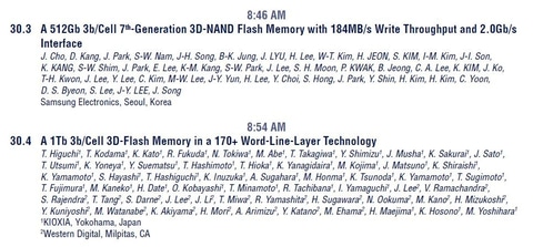
Samsung Electronics reports 512Gbit flash memory with 7th generation 3D NAND technology (lecture number 30.3). The number of stacked memory cells is expected to exceed 160. The TLC method was adopted for multi-valued memory. The write throughput is as high as 184MB / s.
Kioxia and Western Digital have developed a 3D NAND flash technology with more than 170 memory cells stacked (lecture number 30.4). The storage capacity of the prototype silicon die is 1 Tbit. Multi-value storage is TLC method. The storage density is as high as 10.4 Gbit / mm2.
In addition to the above, there are many interesting presentations at the technical lectures at the main event. For details, I would like to report again in the post-live report, so please look forward to it.
